~4 meetings
Integrated MOS amplifiers are probably the most common and highly important devices in majority of analog- or mixed-signal integrated circuits. Wherever analog signals are in place, an OPAMP (OPerational AMPlifier) plays key rule in amplifying, filtering, and further signal processing. In this session, you will learn how to use SpiceOPUS to simulate the overall electrical behaviour of such circuit, including operating point, DC characteristics (differential gain, common mode gain), AC characteristics (gain, phase, bandwidth, margins), transient - time-domain characteristics and noise. As a professional analog circuit designer, you will probably use methods of this session on a regular basis.
First things first - SpiceOPUS and netlists.
In the beginning, you will learn how to describe a circuit in a Spice-friendly input format. Circuit is typically described in a form of a file, called netlist. The structure of a file is like follows:
Circuit name
circuit_description
.control
NUTMEG_commands
.endc
.end
The first line (Circuit name) is never interpreted. circuit_description is the actual description of circuit topology and parameters. You will practice this part on the first meeting. .control is a command, that tells Spice that circuit description is over. NUTMEG_commands are commands that execute various types of analysis. .endc tells Spice that command block has ended, and .end marks the end of a netlist. You can create a netlist file simply by using plain-text editor. (Yes, also various GUI methods exist - with drawing the scheme and then converting it to a netlist. However, it is important for us, the future engineers, to deeply understand the creation of netlists. We will use GUI methods later in exercises.) Typical netlist filename extension is .cir (you will also encounter netlist filename extensions .inc and .lib, but do not worry about those just yet).
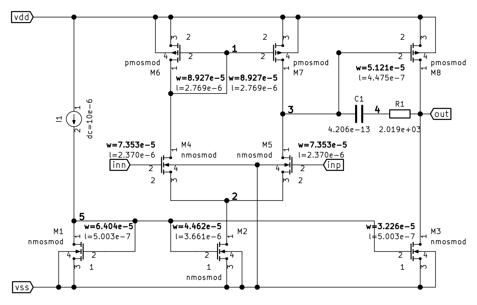
Since the first session is about MOS amplifier, lets take a look on how a single MOS transistor is being described in a netlist. For example, this is how transistor M4 is correctly described:
m4 (1 inn 2 vss) nmosmod w=7.353e-5 l=2.370e-6 m=2
This is maybe a complex beginning, so let us shortly explain this SPICE description (a line started with a star (*) is treated as commentary in SPICE):
* NMOS Transistor
*   _device_name            _model_name
*  /                       /            _model_parameters
* /   connected_nodes     /            /
*/  |-----------------|   |     /---------------------\
*|  \D   G    S    B  /   |     width[m]   length[m]  multiplication
 m4 (1   inn  2   vss ) nmosmod w=7.353e-5 l=2.370e-6 m=2
We named a MOS transistor m4 (the first character m encodes a MOS transistor and the following number/character distinguishes one transistor from another). What follows next, are node names (usually in brackets, but not necessarily). When building a netlist, we have to come up with names for every existing node in our circuit. Having NMOS, node names follow this order - drain, gate, source and bulk node. We assigned the drain pin to circuit node 1, gate to node inn, source to 2 and bulk to vss. Further we have to declare, which model will be used to present the NMOS. In our case, the model name is nmosmod. What follows are numerical parameters, in our case transistor's gate width and length (in meters), and multiplication factor (parallel instances of the same device). Here is an example for PMOS:
* PMOS Transistor
*   _device_name            _model_name
*  /                       /            _model_parameters
* /   connected_nodes     /            /
*/  |-----------------|   |     /---------------------\
*|  \S   G    D    B  /   |     width[m]   length[m]  multiplication
 m6 (1   1   vdd vdd)    pmosmod w=8.927e-5  l=2.769e-6  m=2
Important: m_ transistors have a model name given in our description. Model must be given as an external file. In our case, we can create or download a model library into the same folder as your circuit description file.
Include this into your netlist file (somewhere before circuit description):
.lib 'cmos180n.lib' tm
Now simulator will know, what models to apply for your transistor.
Here is an example of MOSFET part of the circuit description:
    ****************************************
    *180nm OPAMP description
    ****************************************
    * MOSFETS *
    m1 (5 5 vss vss) nmosmod w=6.404e-5 l=5.003e-7 m=1
    m2 (2 5 vss vss) nmosmod w=4.462e-5 l=3.661e-6 m=1
    m3 (out 5 vss vss) nmosmod w=3.226e-5 l=5.003e-7 m=1

    m4 (1 inn 2 vss) nmosmod w=7.353e-5 l=2.370e-6 m=2
    m5 (3 inp 2 vss) nmosmod w=7.353e-5 l=2.370e-6 m=2

    m6 (1 1 vdd vdd) pmosmod w=8.927e-5 l=2.769e-6 m=2
    m7 (3 1 vdd vdd) pmosmod w=8.927e-5 l=2.769e-6 m=2

    m8 (out 3 vdd vdd) pmosmod w=5.121e-5 l=4.475e-7 m=2
    ****************************************
A resistor, for example, is easier to encode:
*  _resistor_name
* / /nodes\  _resistance[ohms]
*/  \     / /
 r1 (out 4) r=2.019e+03
Your first task will be to encode the whole OPAMP circuit in this manner.
We will create a similar circuit as presented in a scheme below. We will also add power supply and signal-source elements to bring this circuit into life.

We did not mention yet, how to load a netlist into the simulator. SpiceOPUS is a command-line tool. When in SpiceOPUS, you have to either navigate to a directory, containing netlist using cd command (see basic Linux Shell / Microsoft Command Prompt commands) or provide full path to a netlist. A keyword source must be given first:
source C:/path/to/the/netlist.cir
The file netlist.cir should be loaded into the SpiceOPUS right away. All NUTMEG commands (the ones between .control and .endc) will be executed as well. If this command executes without errors, you encoded the circuit correctly.
OP Analysis
Operating Point (OP) Analysis is the most basic simulation of a circuit behavior. You will learn how to check if the circuit is alive using OP analysis.
In OP analysis all capacitors/inductors, behave as open/short circuits. If voltage/current sources are specified with a sort of transient waveform, the initial value (time=0) is used. We can run the OP analysis simply by calling:
op
somewhere after the .control sentence. The purpose of OP analysis is basically to find out, what are the initial, starting properties of a simulated circuit. For example, we can check what kind of voltage our OPAMP will produce on the output, considering initial conditions. We can put this line after op:
print v(out)
print will put the result of the expression on the right to display (terminal), so we will be able to read it. v(out) will return absolute electrical potential of node out in voltages. When no differential voltage between inn and inp is set, the MOSAMP output voltage should be near zero.
Sweep (DC) Analysis is a set of multiple OP analyses, but with some altering parameters. Let's say you want to inspect the dependence of output voltage to the changes on input differential voltage or even power supply - you can use a DC analysis to do that.
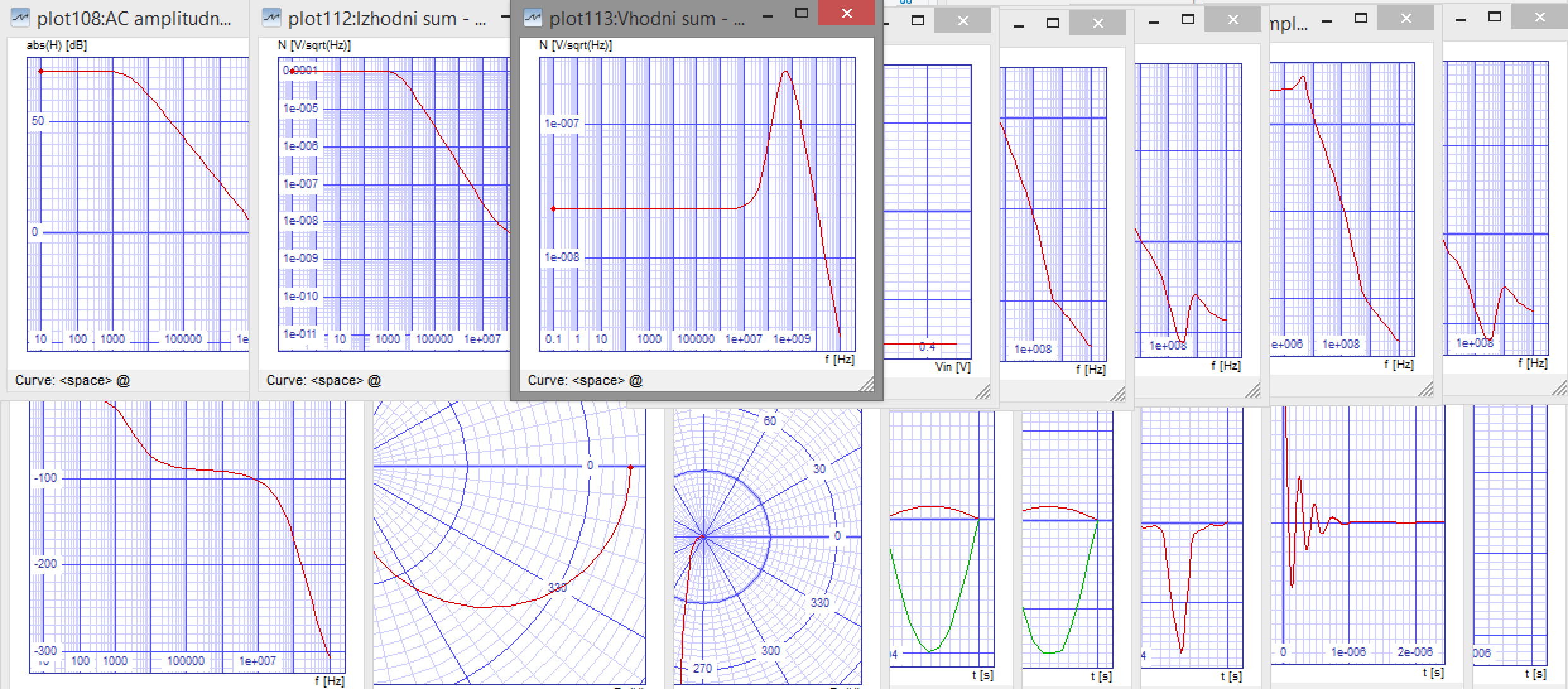
In order to better understand and imagine the simulation results, you will also learn how to plot, interpret and visualize using SpiceOPUS. There is a collage of random fancy plots made using SpiceOpus just below.
Now, let us apply some voltage between the inputs of the OPAMP. We can do the following: we will set the voltage source Vin1 to -1.00 mV, and then with steps of 0.01 mV increase the voltage to +1.00 mV. We can do that with DC analysis:
*      _voltage_source_name
*     /   start
*    /   /  stop
*   /    |  |  step
dc vin1 -1m 1m 0.01m
The DC analysis did execute in the background. If you type display in the Spice command prompt, SpiceOPUS will show you names of vectors and variables, created during various analyses.
Because an "image can speak a thousand words", we will consider plotting the simulated data. Let us make a plot, which will show us how the output voltage changes when applying some differential voltage between the nodes inp and inn on the OPAMP. Let us put it this way:
plot v(out) vs v(inn,inp) xlabel 'v(inn,inp)' ylabel 'v(out)' title 'DC characteristics'
Explanation follows:
*     _data_on_Y_axis
*    /          _data_on_X_axis
*    |         /           _|->the rest is more/less self-explaining
*    |         |          /
plot v(out) vs v(inn,inp) xlabel 'v(inn,inp)' ylabel 'v(out)' title 'DC characteristics'
Spice will produce a plot, similar to this (note that this plot is based on a simulation of open-ended amplifier, i. e. without R2 in the feedback):
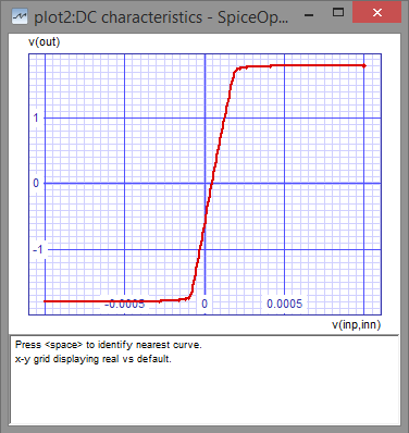
We can see, that output voltage is limited both on top and bottom - this is the OPAMP supply voltage. The slope represents the open-end voltage amplification (also gain). In this case, gain is very high, approx. 13000 V/V, this is
Keep in mind that this is so called open-ended circuit which is not used very often as an amplifier. More often a circuit with a feedback is used, which provides lower gain, but better frequency dependence and stability. We will make our hands dirty simulating such amplifier at the end of this session.
Cursors in SpiceOPUS
In SpiceOPUS, we can use cursors to measure things in output plots and vectors. Cursors are bassically indexes of vector values. The bellow example shows, how to measure DC gain with cursors.
echo 'DC gain measurement'
let c1=0
let c2=0

*     _another word for index of a vector
*    /     _index where...
*   /     /  _in_this_direction...
*  /     /  /     _this_vector...
* /     /  /     /          _reaches this value
*/     /  /     /          /
cursor c1 right v(inn,inp) 0
cursor c2 right v(inn,inp) -0.1m
let gain=(v(out)[%c2]-v(out)[%c1])/(v(inn,inp)[%c2]-v(inn,inp)[%c1])
print gain db(gain)
AC Analysis
We are often curious about how does a circuit respond to signals with various frequencies. In small signal analysis (AC Analysis) Spice can evaluate the circuit's frequency response. In order to execute an AC analysis, we have to choose an input signal source. We will set an ac parameter to a voltage source this way:
*                     _set ac to 1 for ac analysis
*                    /
vin1 (in inp)  dc=0 ac=1
All other existing signal sources are turned off (voltage sources are represented by short circuits, current sources by open circuit). The number 1 in ac=1 actually means peak-to-peak sinusoidal excitation level in volts. Recalling how much gain does our OPAMP produce, the p-p output voltage should be around 13 kV. That is, of course, unreal - in best case, we are limited with the voltage of power supply. However, when simulating a circuit using AC analysis in Spice, all elements are linearized - idealized in a view. Using AC analysis, we are interested more in ratios between signals (gain), than absolute values. We must look on ac=1 as a standard way to turn the voltage source ON and ready for AC analysis.
Let us run the AC analysis:
*     _frequency_unit_(decade)
*    /   _points_per_freq_unit
*   /   /  _start_freq
*  /   /  /  _stop_freq
ac dec 10 10 1G
The result of AC analysis are vectors that contain as many components as there were frequencies. All resulting vectors are complex, hence have the real and imaginary component (amplitude and phase). Now let us consider the following lines in .control block:
let h=v(out)/v(inn,inp)
let hmag=db(h)
let hphase=unwrap(ph(h))
let will create a new vector h. Spice lets us to calculate the ratio between two existing vectors, in this case v(out)/v(inn,inp), and store it in h. Now we will firstly extract the magnitude part of the frequency response in decibels hmag=db(h) and then the phase part in degrees hphase=unwrap(ph(h)). While phase is typically in the range of 0 to 2*PI, the unwrap() function unwraps the phase vector to extend through a larger range. We can now have two separate plots - amplitude and phase:
*      _vector_to_plot - already contains the frequency scale (Y axis)
*     /
plot hmag   xlabel 'f [Hz]' ylabel 'abs(H) [dB]' title 'AC amplitude plot'
plot hphase xlabel 'f [Hz]' ylabel 'ph(H) [deg]' title 'AC phase plot'
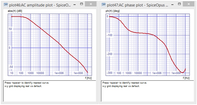
We assume you already know how to read those two graphs, but nevertheless: at frequency 10 Hz, where AC analysis started, the OPAMP produces 82 dB of gain but drops towards 50 dB at about 10 kHz, and to 0 dB gain near 3 MHz. The phase plot is more diverse, signals at 10 Hz have 0 degrees of phase shift. With increasing frequency the signal "delay" increases as well, firstly to -90 degrees phase shift and then drops even more. We need those plots to understand how magnitude is changing with frequency and how stable is the OPAMP's output. We will learn also how to find the famous -3 dB point, and calculate standard stability margins (gain at 180 degrees and phase margin 180-phase at 0 dB point) using Nutmeg commands.
A good way to see, whether an OPAMP output is stable (does not oscillate) is so called polar plot. Let us see how to draw such a plot in Spice:
*                       _complex_polar_plot option
*                      |-----------|
plot v(out)/v(inn,inp) mode cx polar xlabel 'Re(H)' ylabel 'Im(H)' title 'Polar diagram'

* zoomed view:               x_axis_limits_   _y_axis_limits
*                                    |-----| |-----|
plot v(out)/v(inn,inp) mode cx polar xl -2 2 yl -2 2 xlabel 'Re(H)' ylabel 'Im(H)' title 'Polar diagram'
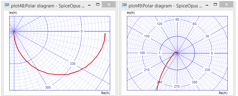
While the polar plot does not encircle -1+0j we consider the OPAMP stable.
NOISE Analysis
Often engineers are interested in information about signal noise the circuit will produce. Some electrical components produce a significant (measurable) amount of noise, which is further added to a signal. We can simulate that as well with SpiceOPUS.
*        _output_voltage_of_interest
*       /         _independent_voltage/current_source
*      /         /
*     |-------|  |   |---> same as for AC analysis
noise v(out, 0) vin1 dec 10 0.1 100G 1
*this is to access noise spectrum densities in previous namespace:
setplot previous

plot sqrt(onoise_spectrum) ylog xlabel 'f [Hz]' ylabel 'N [v/sqrt(Hz)]' title 'Input noise'
plot sqrt(inoise_spectrum) ylog xlabel 'f [Hz]' ylabel 'N [v/sqrt(Hz)]' title 'Output noise'
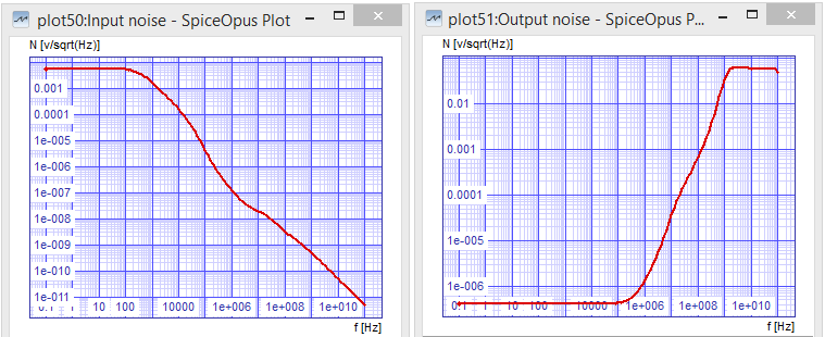
The input noise spectrum represents the noise that must be fed into an ideal circuit (with no noise) in order to produce the same output noise spectrum as the real-world circuit does.
Subcircuit
Now, the OPAMP is a compact circuit, that can be used in many ways and will not often be altered in the future of this session. This is why we will enclose the OPAMP in an so-called sub-circuit. This will help us handle the OPAMP circuit more easily when using it in various setups. This is how we encapsulate an existing netlist into a sub-circuit:
*            _sub-circuit_name
*           /        _nodes-to-be-accessible-from-the-outer-world
*          /        /
*         /    /------------------/
.subckt mosamp inp inn out vdd vss
m2 (2 5 vss vss) nmosmod w=4.462e-5 l=3.661e-6 m=1
m1 (5 5 vss vss) nmosmod w=6.404e-5 l=5.003e-7 m=1
*               .
*               .
*               .
.ends
* \
*  \_keyword for ending sub-circuit
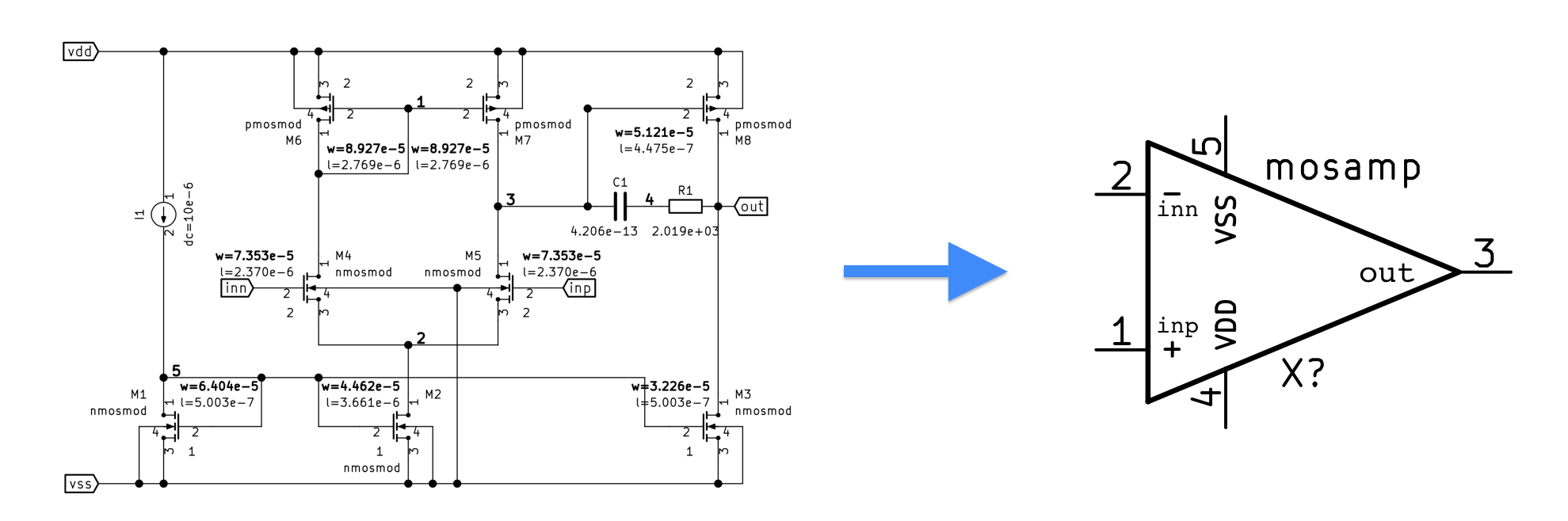
We can now use the sub-circuit, named mosamp in another circuit.
*   _device_instance_name
*  /  _circuit_node_names (mind the node order in the sub-circuit)
* /  /                        _sub-circuit_name
*/  /-------------------\    /
x1 (inp inn outop vdd vss) mosamp
20 dB Amplifier Using Integrated OPAMP - Various Analyses
Until now, we thought about the OPAMP as an independent component. Such open-ended OPAMP is not very useful for analog signal amplifying - it has several disadvantages, for example: extremely high voltage gain causes having output often in saturation and it has narrow operational bandwidth.
We will now consider the circuit from the image of an OPAMP, drawn together with peripheral circuitry (power supply, R1, R2, Vin1, Vcom1, Cl1). This is a topology of a well known Inverting Amplifier. Our first task will be to repeat the DC analysis, observing v(out) in relation to v(inn, inp).
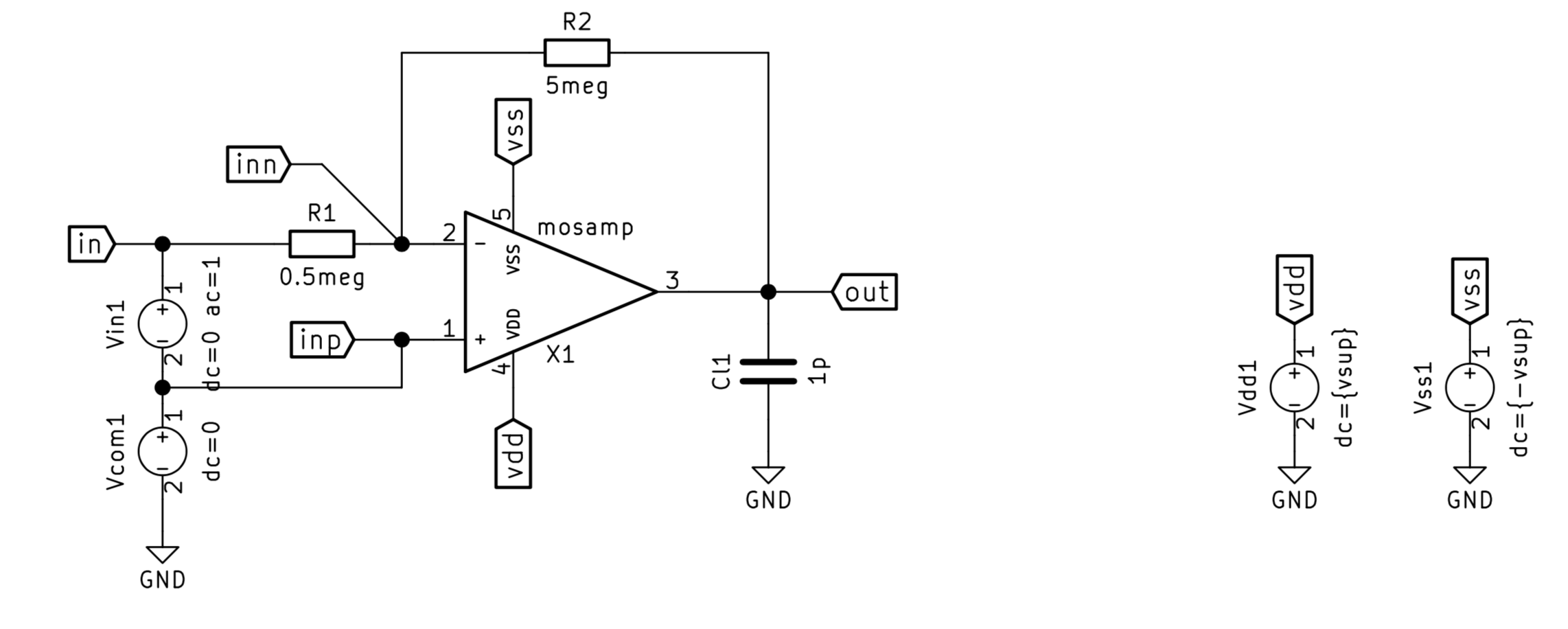
dc vin1 -0.5 0.5 0.005
plot v(out) xlabel 'Vin [V]' ylabel 'Vout [V]' title '20dB gain'
Note a small difference between DC analysis command in the previous case - there is no keyword vs and no explicit x axis data. With DC analysis, we altered vin1 voltage source, so this is our default x axis vector. The same result would be given with calling DC analysis as: plot v(out) vs v(in, inp) xlabel ... Graphic plot is as follows:
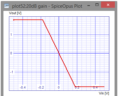
You will notice that maximal and minimal output voltages are again limited by power supply voltage. The output voltage is now decreasing with increasing differential voltage (inverting amplifier). The slope is much lower than in open-ended case, i.e. lower voltage gain (i.e. 20 dB). Although gain is now significantly lower, we will observe that bandwidth is significantly larger - this circuit can uniformly amplify much larger signal spectra:
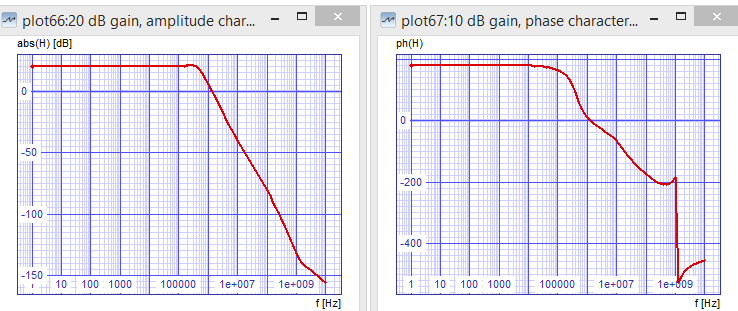
ac dec 10 1 10G
let h = v(out)/v(in)
plot db(h) xlabel  'f [Hz]' ylabel 'abs(H) [dB]' title '20 dB gain, amplitude characteristics'
plot unwrap(ph(h)) xlabel 'f [Hz]' ylabel 'ph(H)' title '10 dB gain, phase characteristics'
Transient analysis
As engineers, we are often interested in signals in time-domain, for example, how does output voltage change in time. Let us equip our differential input voltage source Vin1 with a sine generator like this:
*                       damping_factor_
*                  delay_to_start____  \
*             frequency[Hz]________  \  \
*          half_amplitude_______   \  \  \
*     signal_offset__________   \   \  \  \
*                            \   \   \  \  \
vin1 (in inp)  dc=0 ac=1 sin=(0 0.05 1k  0  0)
Let us run the transient analysis and plot the results. We have to provide time-step in seconds, stop time and (optionally) the start time:
*      _step
*     /     _stop
*    /     /    _start
tran 0.01m 4.5m 3m

*     _shown on same plot
*    |----------|
plot v(in) v(out) xlabel 't [s]' ylabel '[V]' title '20 dB amp., sine response'
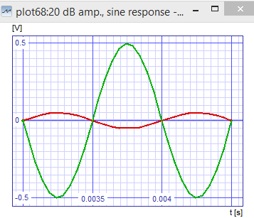
The red-colored sine graph is the input signal (signal generated by Vin1). Green-colored sine is the amplified signal v(out). It is ten times larger than the input signal, which is 20 dB.
We usually want the output signal so be only amplified but not altered in other ways - signal shape must remain unchanged after amplification. We can measure the signal distortion using Fourier analysis.
* Uniformly linearize scale on time axis:
linearize 0.01m
* Run the fourier analysis and display results:
*         _fundamental_frequency
*        /   _output_signal
*       /   /
fourier 1k v(out)
The outcome should be something like this:
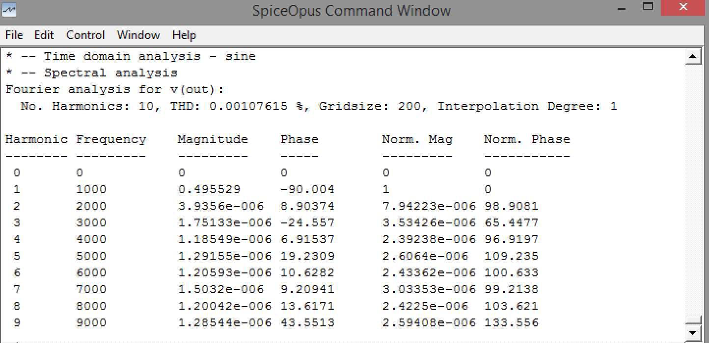
The number that tells us how badly the output signal is distorted, is THD or Total Harmonic Distortion which is around 0.001 % for this circuit. This is a very low amount of distortion. You can experiment how to get a more distorted signal. For example, you can enlarge the input signal from 0.05 V to 0.3 V and see what happens. You can correct the second argument when setting the sine generator on Vin1, or you can do that also after the .control block, just before running the fourier again with:
* Change a parameter in the circuit "on the fly":
*       _at_vin1_change_property:
*      /    _property
*     /    /    _argument_number (1 for the second)
*    /    /    /   _value
let @vin1[sin][1]=0.3
Running fourier 1k v(out) again you should see how THD goes crazy.
We will also play around with stability of the OPAMP in this session. One of the methods to inspect whether the circuit is stable is to apply a very steep pulse on the input. If the output starts to oscillate, than the OPAMP needs to be additionally compensated. This is how we apply the pulse using voltage source Vin1:
*      _at_vin1_change_property:
*     /    _property
*     |   |           _start_voltage
*     |   |          /   _stop_voltage
*     |   |         /   /   _time_delay
*     |   |        /   /   /   _time_to_stop_voltage
*     |   |       /   /   /   /
let @vin1[pulse]=(0;0.05;1n;0.1n)

* Additional possible parameters for pulse generator (in this order):

*   _time_to_first_voltage (falling time)
*  /    _pulsewidth (time between end of rise and start to fall)
* /    /    _period (repeat time)
We will practice those methods on our laboratory sessions.