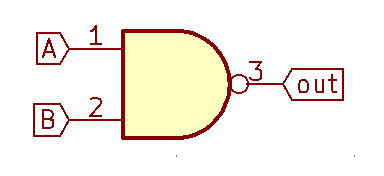
NAND gate (NOT-AND) is a logical gate which outputs false only if both inputs are true:
* NAND LOGICAL TABLE *
* a b * out
***********
* 0 0 * 1 *
* 0 1 * 1 *
* 1 0 * 1 *
* 1 1 * 0 *
***********
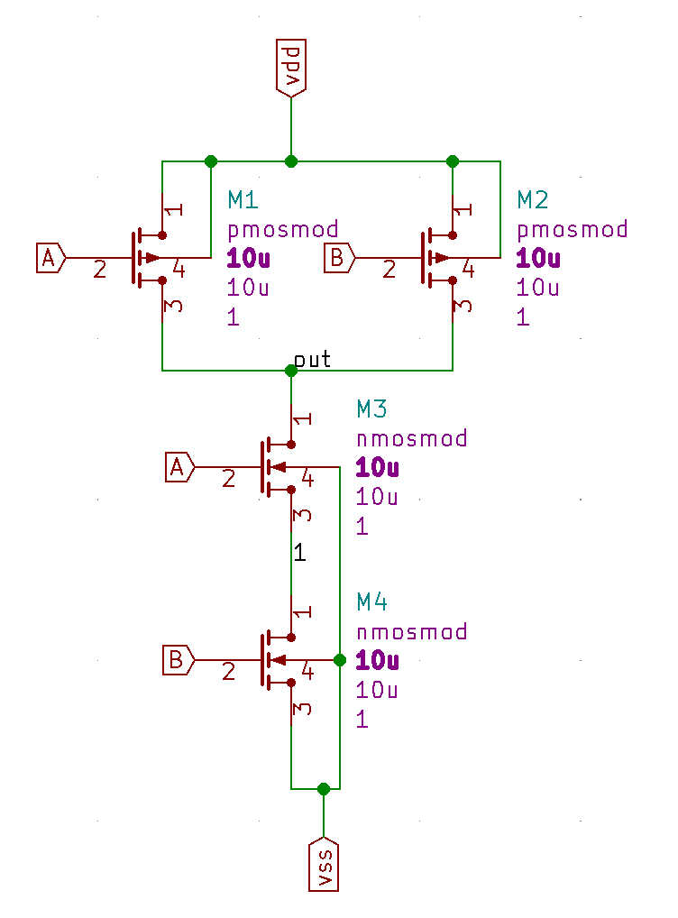
We can implement a NAND gate using the following schematics. Please use models from the previous exercise.
.lib 'cmos180n.lib' tm

* NAND logic gate
*********************************************************
*   D G  S   B for nmos
m3 (out a 1 vss)    nmosmod w=10u  l=10u  m=1
m4 (1 b vss vss)    nmosmod w=10u  l=10u  m=1

*   S G D B for pmos
m1 (vdd a out vdd)    pmosmod w=10u  l=10u  m=1
m2 (vdd b out vdd)    pmosmod w=10u  l=10u  m=1
*********************************************************
We have to add power supply and signal inputs as well.
* Logic input
va (a 0) dc=0
vb (b 0) dc=0

* Power Supply
vdd (vdd 0) dc=1.5
vss (vss 0) dc=-1.5
We can check the NAND truth table now. Remember, that logical 1 in this technology (using positive and negative supply) is 1.5 V and logical 0 is -1.5 V.
.control
echo Operating point va=vb=0
op
print out

echo OP Analysis va=-1.5 vb=-1.5
let @va[dc]=-1.5
let @vb[dc]=-1.5
op
print out

echo OP Analysis va=-1.5 vb=1.5
let @va[dc]=-1.5
let @vb[dc]=1.5
op
print out

echo OP Analysis va=1.5 vb=-1.5
let @va[dc]=1.5
let @vb[dc]=-1.5
op
print out

echo OP Analysis va=+1.5 vb=+1.5
let @va[dc]=1.5
let @vb[dc]=1.5
op
print out

.endc
Perform a DC sweep on A or B input and see how output changes. Apply time-domain pulses and observe output.
Half-adder
Now consider a half-adder made only of NAND gates. We need five of them and we will rather not encode them transistor-vise.

Subcircuit
Create a file nand_subckt.cir:
*Empty line

.lib 'cmos180n.lib' tm

*            _sub-circuit_name
*           /         _nodes-to-be-accessible-from-the-outer-world
*                    /(in this order!)
*          /        /
*         /  /--------------/
.subckt nand a b out vdd vss
*   D G  S   B for nmos
m3 (out a 1 vss)    nmosmod w=1u  l=1u  m=1
m4 (1 b vss vss)    nmosmod w=1u  l=1u  m=1

*   S G D B for pmos
m1 (vdd a out vdd)    pmosmod w=1u  l=1u  m=1
m2 (vdd b out vdd)    pmosmod w=1u  l=1u  m=1
.ends
You can now build a higher-level circuit like this:
xnand1 (a b 1 vdd vss) nand
xnand2 (a 1 2 vdd vss) nand
x stands for external subcircuit and is followed by instance name. In parentheses nodes are given - the order corresponds to connections in subcircuit definition (1 in higher level circuit is connected to out in NAND subcircuit.
For example, xnand2 has signal a connected to its internal a input, signal from node 1, connected to its internal b and node 2 is connected to NAND internal out.
Our half-adder can now look like:
.include  'nand_subckt.cir'

* NAND logic gate
*********************************************************
* a device beginning with x -> external -> subcircuit
xnand1 (a b 1 vdd vss) nand
xnand2 (a 1 2 vdd vss) nand
xnand3 (1 b 3 vdd vss) nand
xnand4 (2 3 sum vdd vss) nand
xnand5 (1 1 carry vdd vss) nand
*********************************************************
* Power Supply
vdd (vdd 0) dc=1.5
vss (vss 0) dc=-1.5
*********************************************************
* Signal/logic input
va (a 0) dc=0
vb (b 0) dc=0
*********************************************************

.end
Where nand_subckt.cir is a file that contains the subcircuit definition, residing in the same folder.
Subcircuits can be parameterized, meaning, they can receive parameters that set up properties of included devices, for example:
.subckt nand_param a b out vdd vss param: wn=2 ln=1 wp=4 lp=1
* NAND logic gate
*********************************************************
*   D G  S   B for nmos
m3  (out a 1 vss) nmosmod w={wn*0.18u} l={ln*0.18u} m=1
m4  (1 b vss vss) nmosmod w={wn*0.18u} l={ln*0.18u} m=1

*   S G  D   B for pmos
m1  vdd a out vdd pmosmod w={wp*0.18u} l={lp*0.18u} m=1
m2  vdd b out vdd pmosmod w={wp*0.18u} l={lp*0.18u} m=1
*********************************************************
.ends
Our nand_param (parameterized NAND) takes four parameters: width of a NMOS wn, length of a NMOS ln, width of a PMOS pw and length of a PMOS lp. When you inspect further, you will see that actual W and L are being calculated with a formula, such as {wn*0.180n}, which basically gives you a multiplication of the smallest possible width in the 180nm CMOS technology.
Using a nand_param subcircuit now creates every NMOS being w={2*0.18u} l={1*0.18u} and every PMOS being w={4*0.18u} l={1*0.18u} .
Now, this will be true for every nand_param used across the circuit definition, that do not have parameters set SPECIFICALLY. In the Half-adder definition, one can set parameters for EACH instance of the NAND gate like this:
* NAND logic gate
*********************************************************
xnand1 (a b 1 vdd vss) nand_param wn=10 ln=10 wp=20 lp=20
xnand2 (a 1 2 vdd vss) nand_param
xnand3 (1 b 3 vdd vss) nand_param
xnand4 (2 3 sum vdd vss) nand_param
xnand5 (1 1 carry vdd vss) nand_param
*********************************************************
Now only xnand1 instance has significantly larger transistors and the rest have their default value, as specified in a subcircuit.
In our LAB session we tested our circuits truth table. Files are available here: